Cjs02-qc18w-v1.3 Best -
Scanner, 3D Analyzer and Monitor - exclusively for Windows 10!
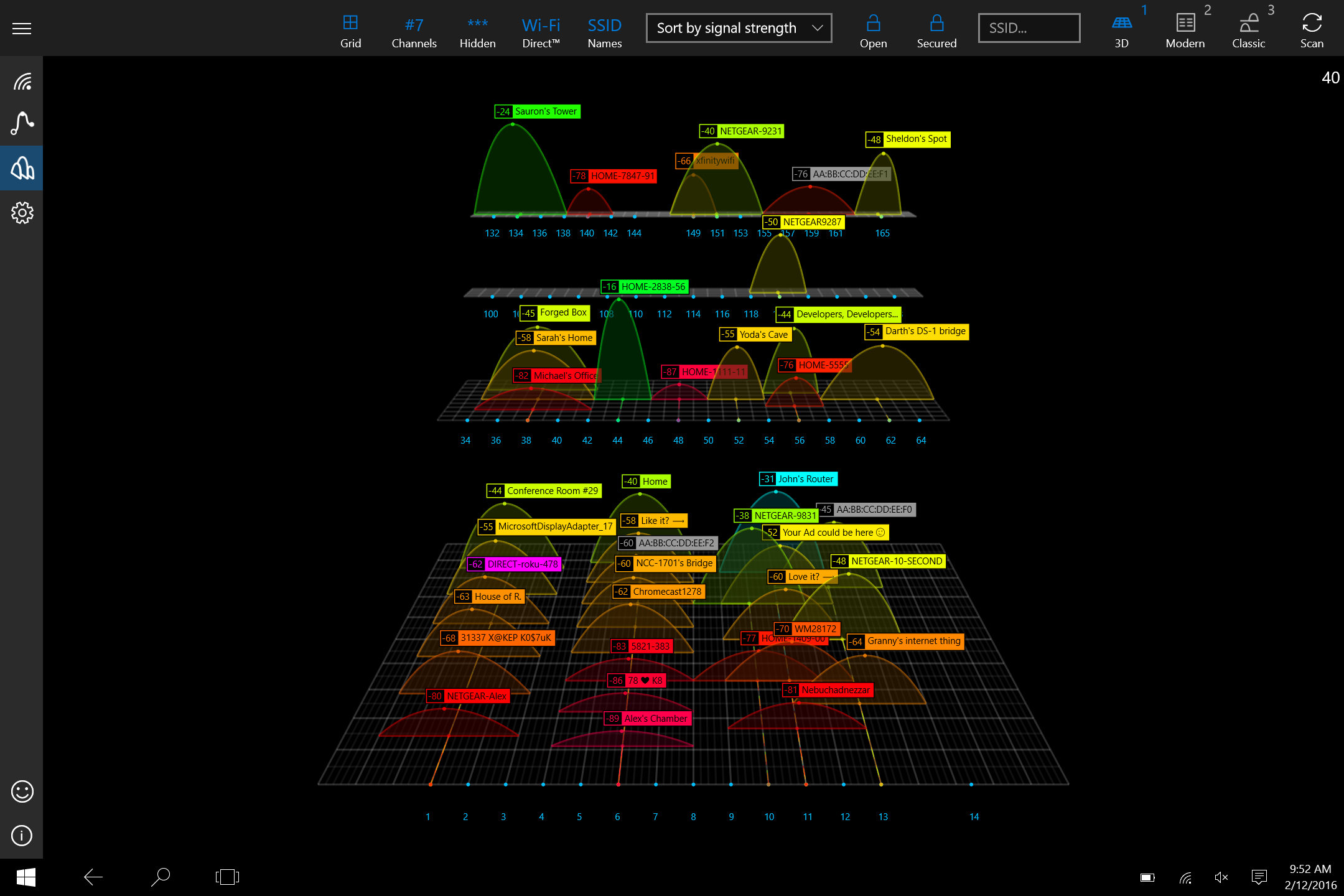
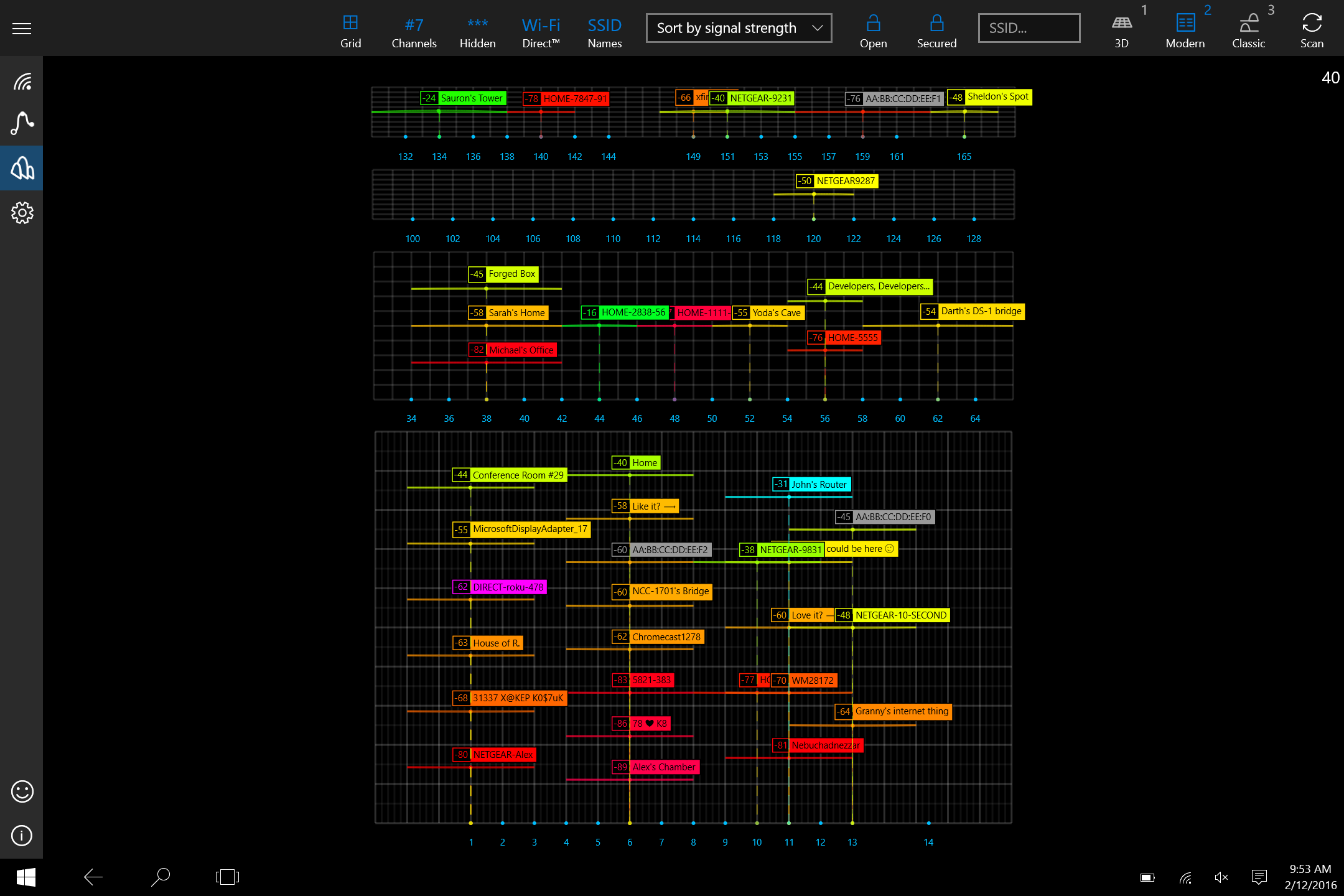
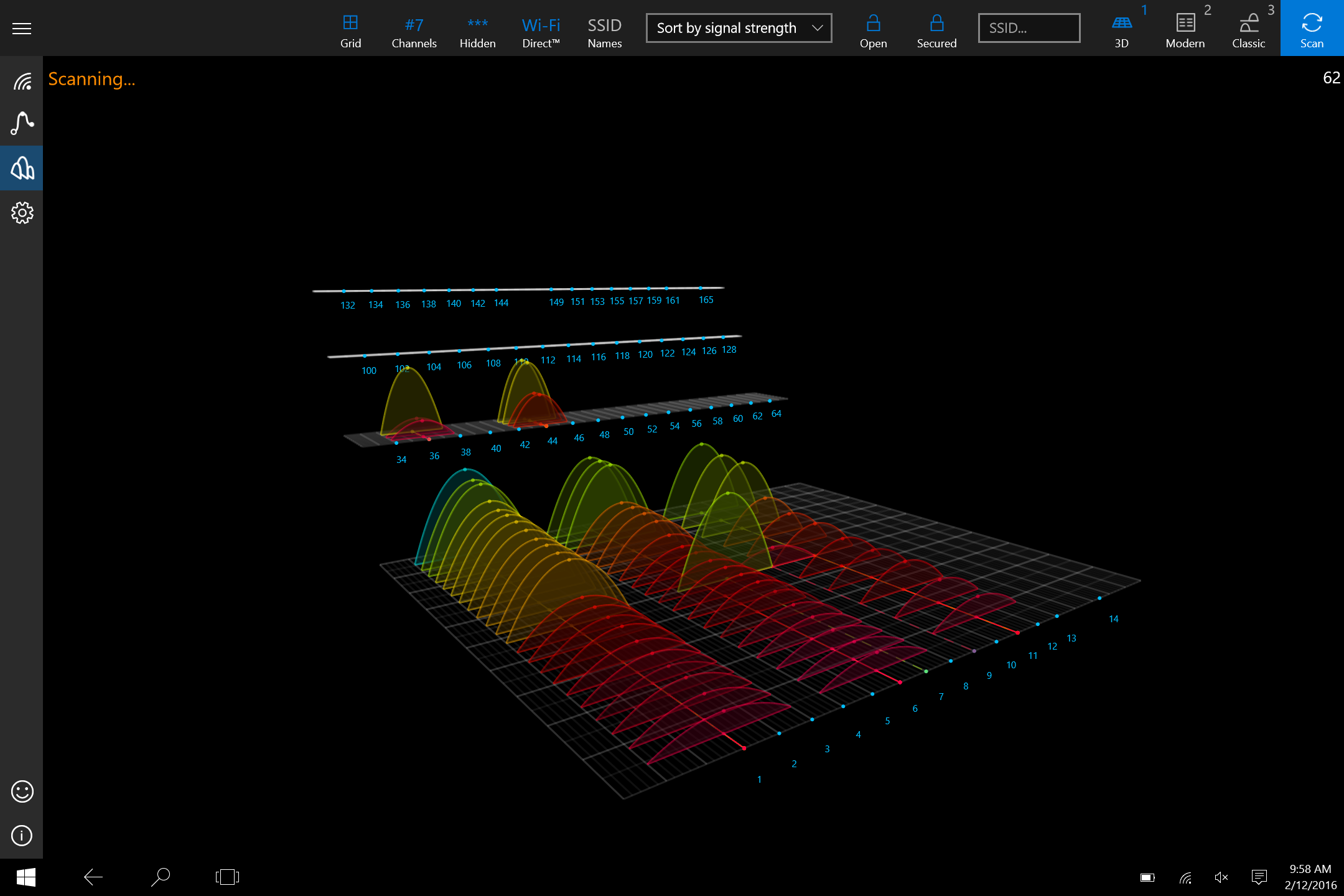
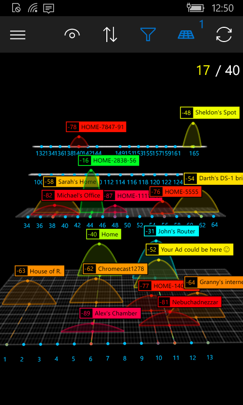
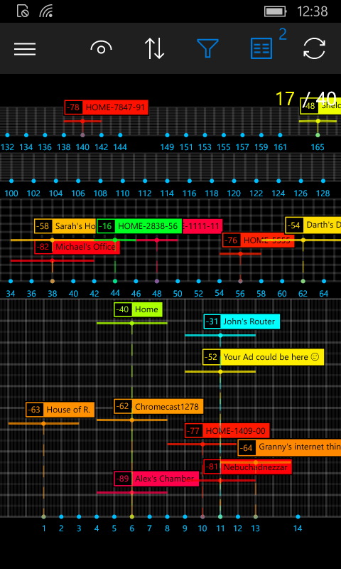
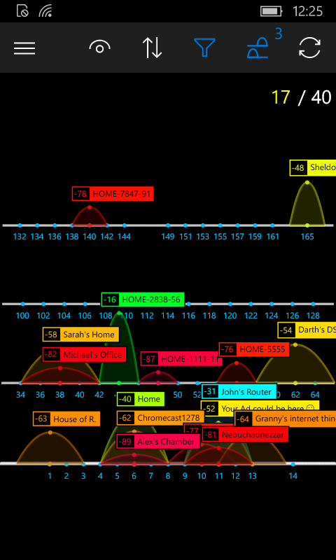
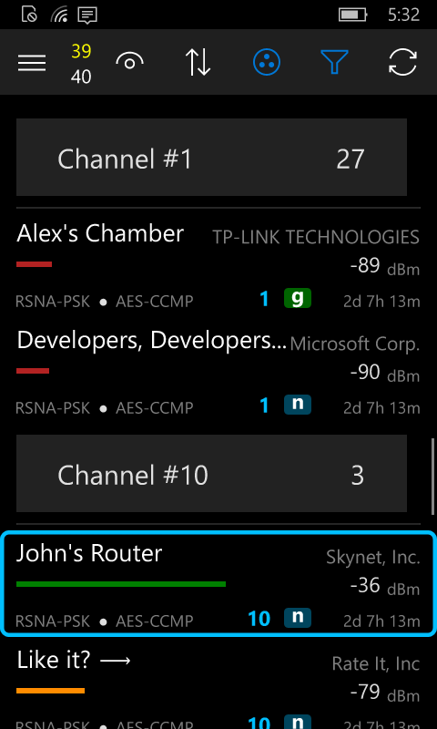
- Scan the space around you for any Wi-Fi networks
- Unique touch-friendly 3D analysis of channel distributions
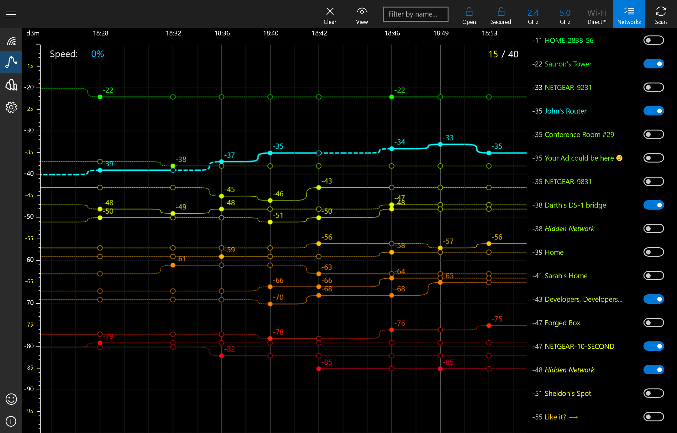
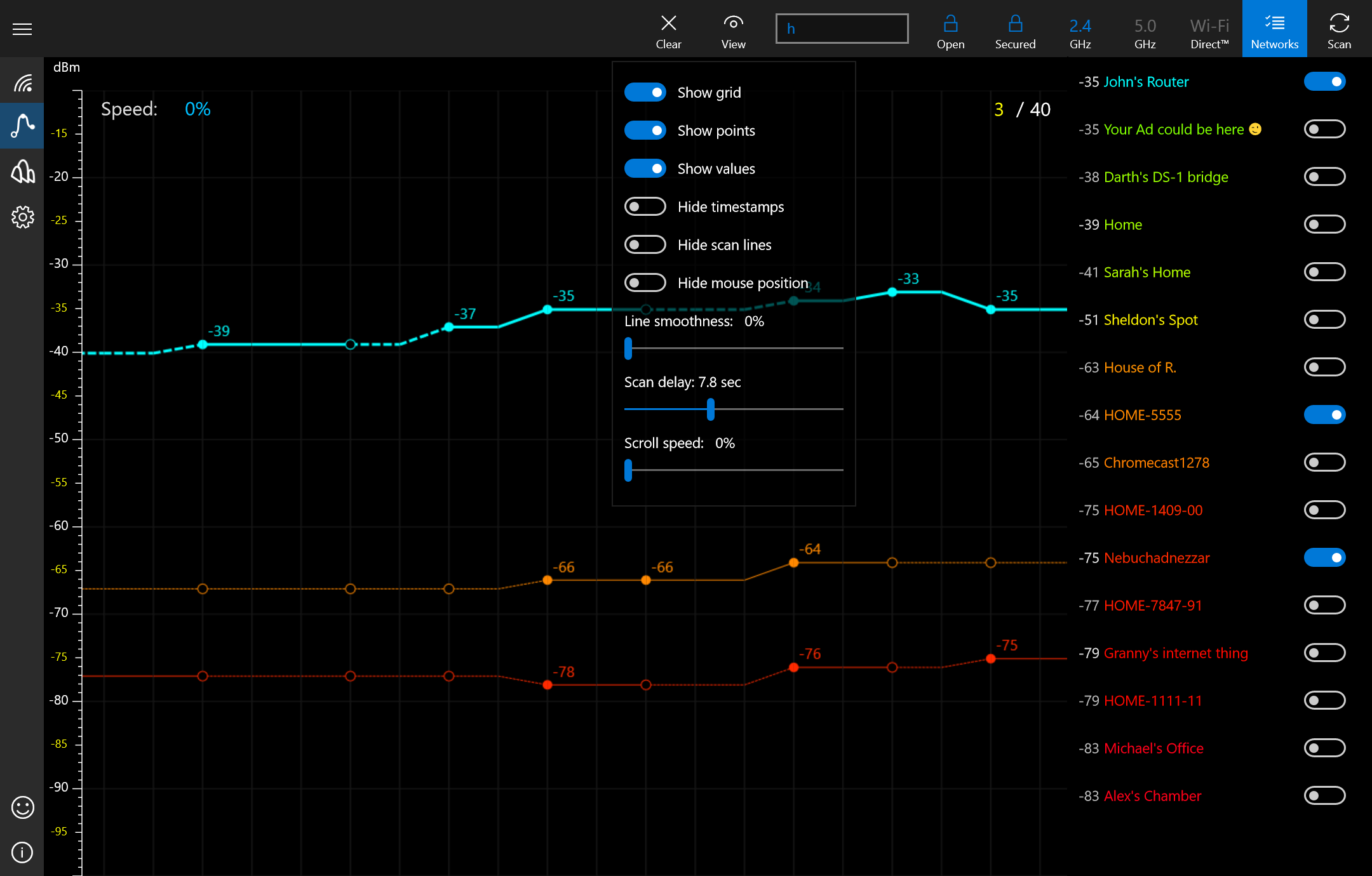
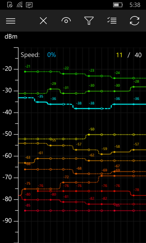
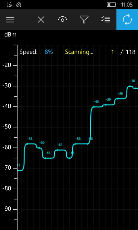
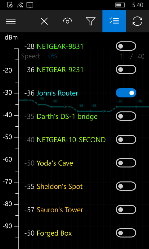
- Unique real time signal level monitor
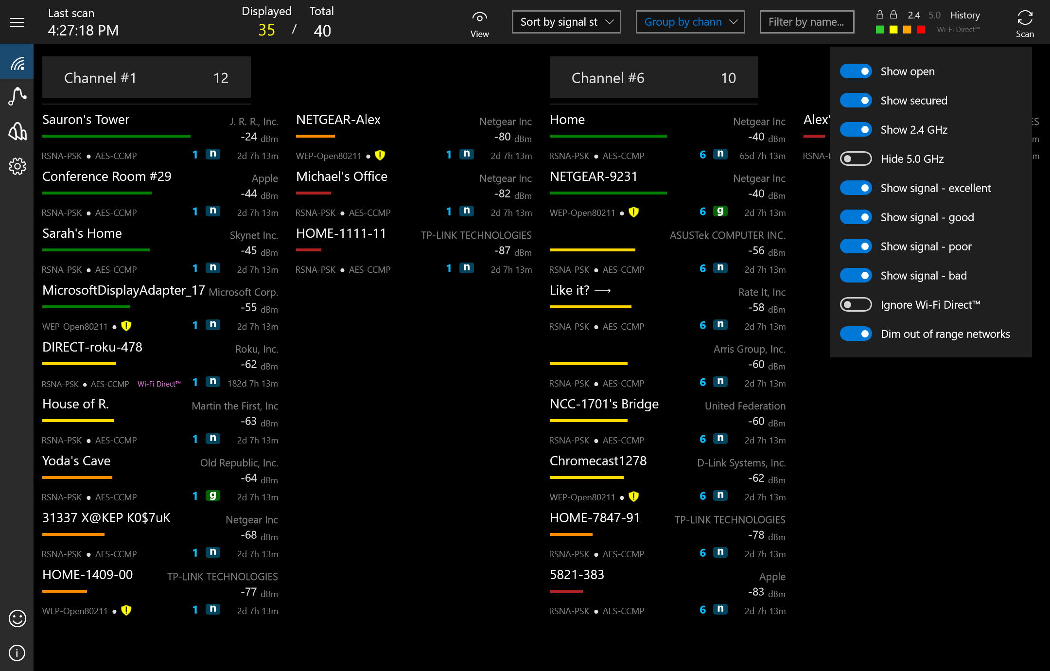
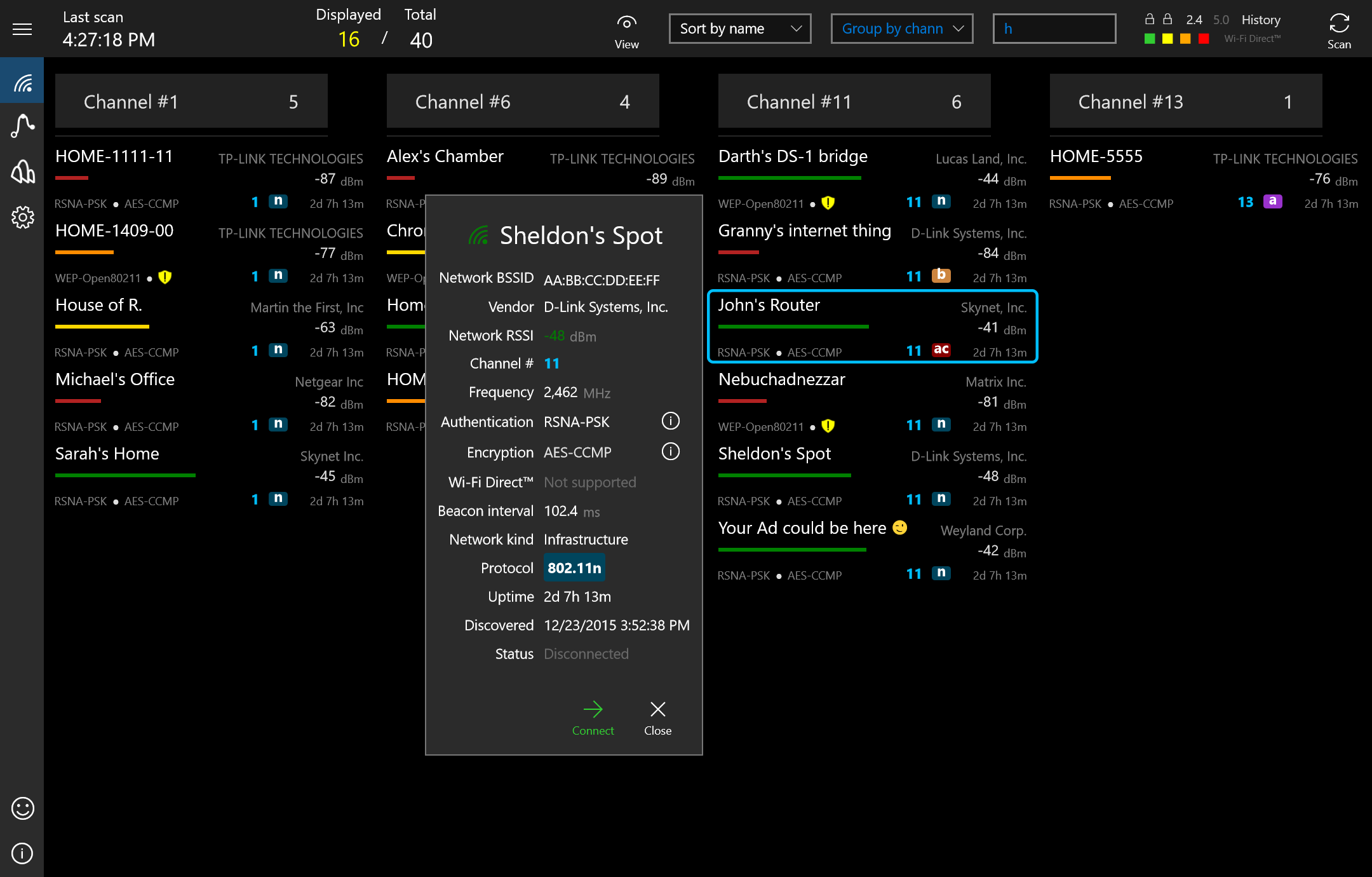
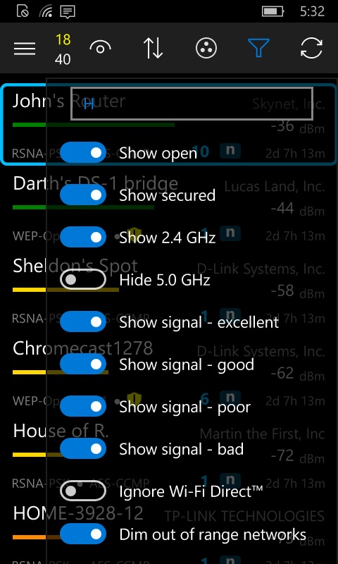
- Filter, sort and group available networks
- Switch between different networks instantly
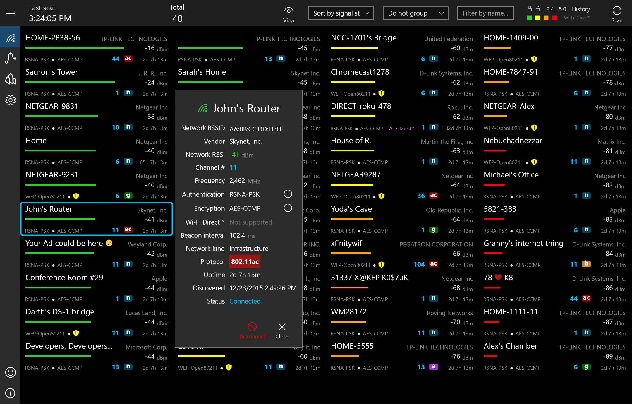
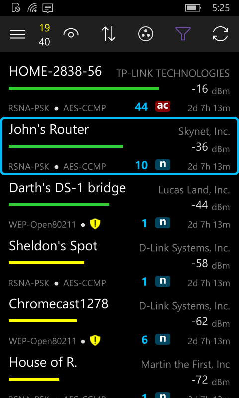
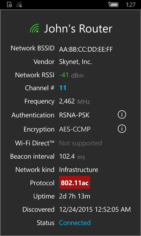
- Detailed info about any Wi-Fi access point (vendor, security, MAC etc.)
- See all Wi-Fi Direct™ capable devices
- Find less used channel for your own router
- Multiple Wi-Fi adapters support
- Small app package - just about 4-5 MB
- No Ads!
Available for

© 2023 Forged Bytes. All rights reserved.